Board Assembly
You are welcomed to come to our factory to buy the latest selling, low price, and high-quality Board Assembly, Hoshineo Lcd-Tech looks forward to cooperating with you.
Send Inquiry
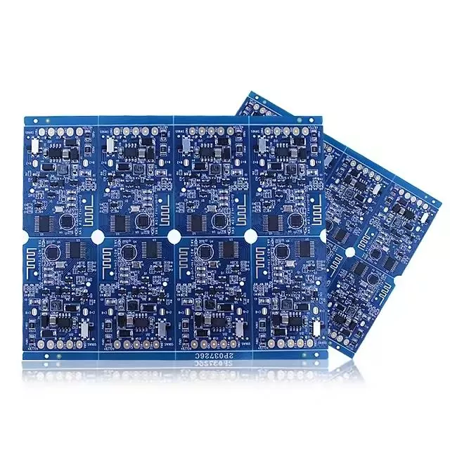
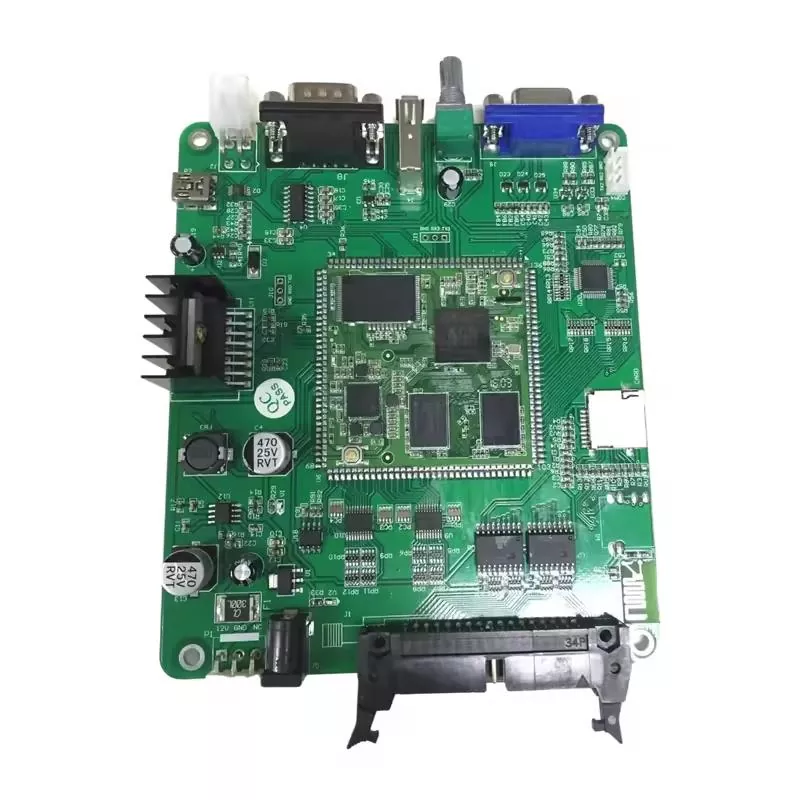
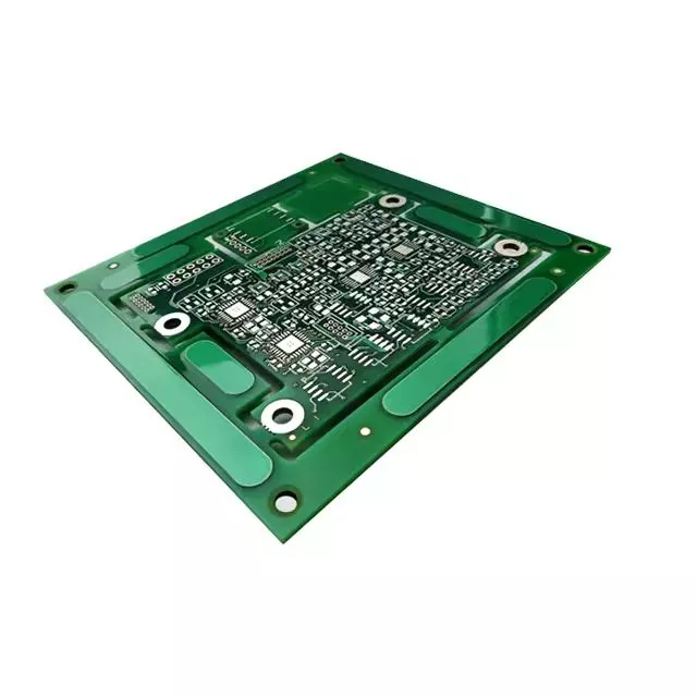
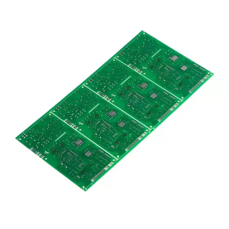
Board Assembly is a process that involves mounting electronic components on a printed circuit board (PCB). The PCB consists of many small electronic components such as capacitors, resistors, and other electronic chips that are soldered onto the board. These components can be pre-soldered or soldered by using pick and place machines. The process of Board Assembly is highly complex and requires a great deal of expertise. Using the right board assembly services is therefore very important.
Hoshineo Lcd-Tech China Anti-Oxidation Gold Finger PCB product parameters:
| ITEMS | Parameter | |||||
| Number of Layers | 1-20 layers | |||||
| Board Materials | FR4,CME3,CME1,5G | |||||
| PCB Size (Min- Max) | 50x80mm to 1000mm×600mm ( 39.37"x23.6") | |||||
| innerlayer line width/space(min) | 4mil/4mil(100um/100um) | |||||
| Finish Plating /Surface Finishes | HASL ,OSP,ENIG,HASL,gold finger,Au Panel,OSP,ENIG | |||||
| innerlayer pad (min) | 5mil(0.13mm) | |||||
| Core thickness (min) | 8mli(0.2mm) | |||||
| Finisher Copper Inner Layers | 1/2oz(17um)a- | |||||
| Finished Copper Outer Layers | 1/2oz(17um) | |||||
| Final PCB Thickness (tolerance %) | 0.5-4.0mm | |||||
| Final PCB Thickness (tolerance %) | Thickness<1.0mm | |||||
| 1.0mm≤Thickness<2.0mm | ||||||
| Thickness≥2.0mm | ||||||
| inner layer process | Brown Oxide | |||||
| Minimum Conductor Space | ±3mil(±76um) | |||||
| Minimum Drill Hole Size | 0.25mm | |||||
| min diameter of finished hole | 0.2mm | |||||
| Hole position accuracy | ±2mil(±50um) | |||||
| Drilled slot tolerance | ±3mil(±75um) | |||||
| PTH tolerance | ±2mil(±50um) | |||||
| NPTH tolerance | ±1mil(±25um) | |||||
| maxA.R.Of PTH | 8:01 | |||||
| PTH hole copper thickness | 0.4-2mil(10-50um) | |||||
| image to image tolerance | ±3mil(0.075mm) | |||||
| Solder Mask Thickness | line end 0.4-1.2mil(10-30um) | |||||
| line Corner ≥0.2mil(5um) | ||||||
| on Substrate | ≤Finished Cu | |||||
| thickness+1.2mm≤Finished Cu | ||||||
| thickness+30um)≤+1.2mil≤+30um) | ||||||
| min solder mask dam | 4.0mil(100um) | |||||
| impedance control and tolerance | 50Ω±10% | |||||
| warp and twist | ≤0.5% | |||||
| Delivery time | 1-2 layers 10-12day | |||||
| 4-20 layers 12-20days | ||||||
| Package | General export packaging | |||||
Hoshineo Lcd-Tech China Anti-Oxidation Gold Finger PCB Feature
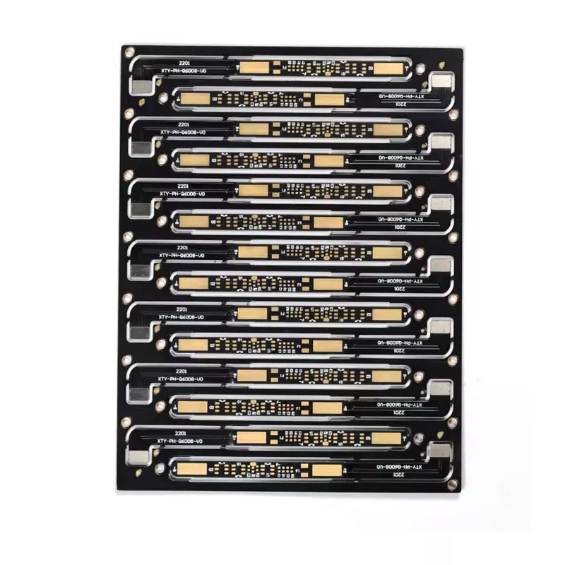
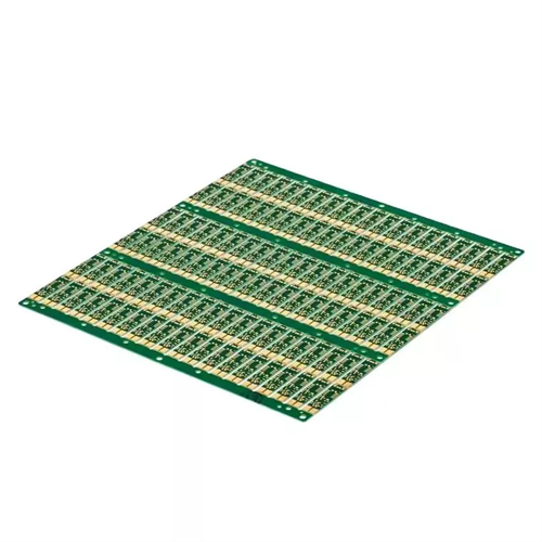
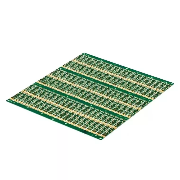
Good electrical conductivity: The gold finger part is usually plated with conductive materials such as gold or nickel gold, which have excellent electrical conductivity and can ensure the accuracy and stability of signal transmission.
Excellent oxidation resistance: Through antioxidant treatment, Anti-Oxidation Gold Finger PCB can effectively prevent the oxidation of copper layer and maintain its good weldability and electrical performance.
Neatly arranged: The pads on the Anti-Oxidation Gold Finger PCB are usually located on the edge of the board and are neatly arranged into a rectangle of the same length and width. This design facilitates docking with the pin of the connector for fast connection and signal transmission.
Various application scenarios: Anti-Oxidation Gold Finger PCB is widely used in fields requiring high reliability and high stability connection, such as computer memory, graphics card, network card, memory, U disk, card reader and other electronic equipment.
Hoshineo Lcd-Tech China Anti-Oxidation Gold Finger PCB Details
Packing & Delivery
Employ thickened plastic vacuum packaging for superior sealing strength and resistance to breakage. The exterior packaging utilizes a 3K-K laminated carton, further reinforced with foam padding for added protection.

