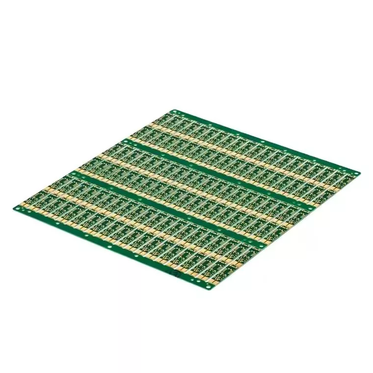
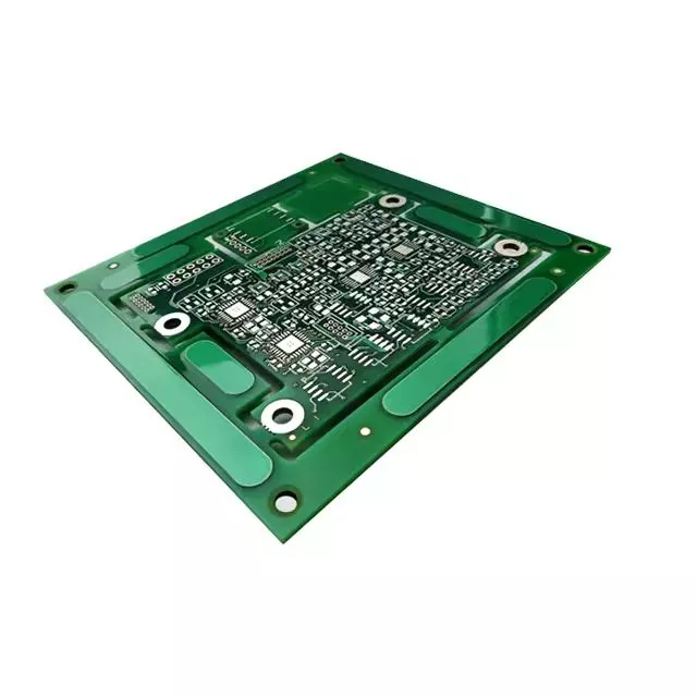
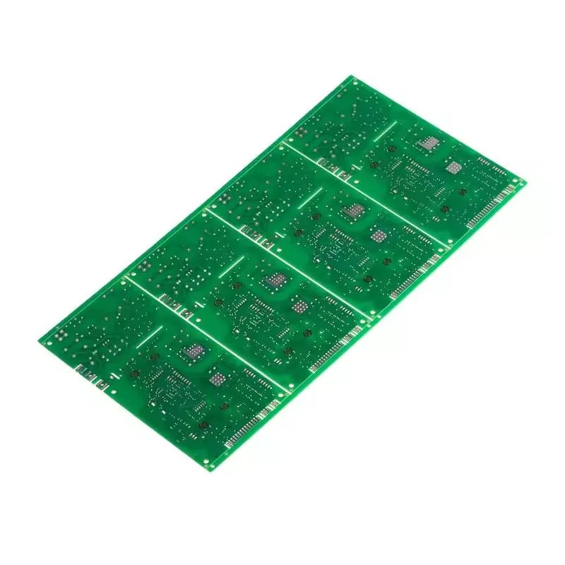
Flex Circuit Board
The producers of Hoshineo Lcd-Tech in China offer high-quality products, you are welcome to purchase straight high-quality Flex Circuit Board at a good price.
Send Inquiry
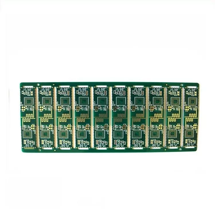
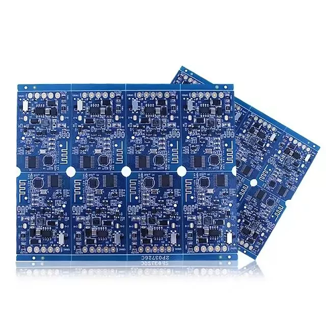
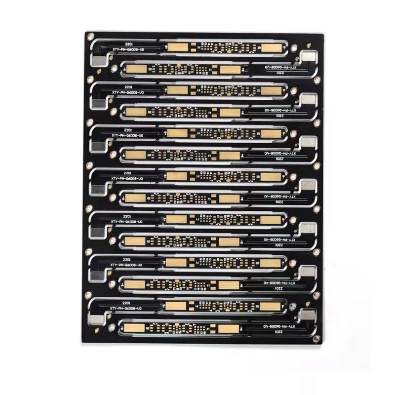
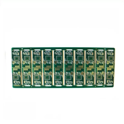
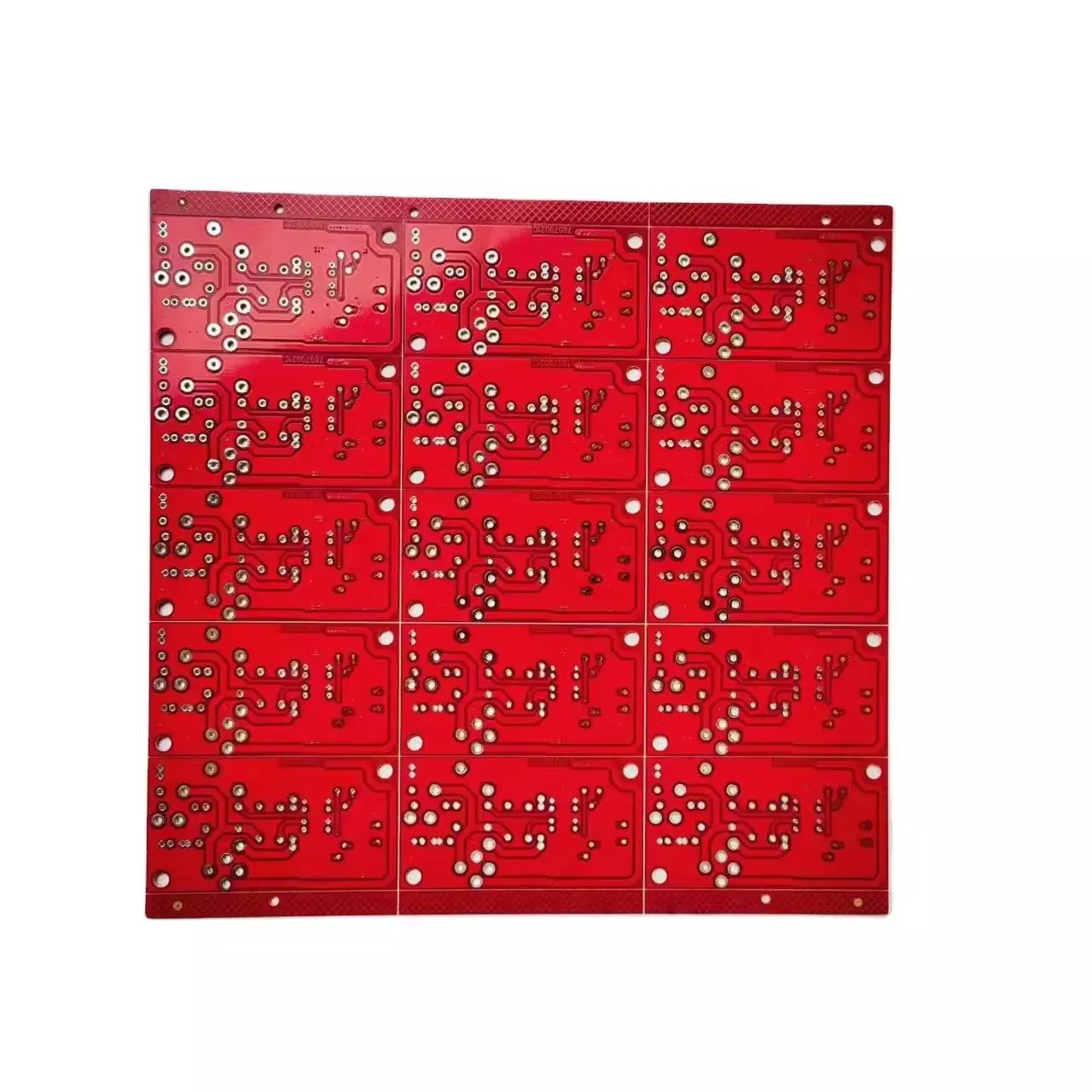
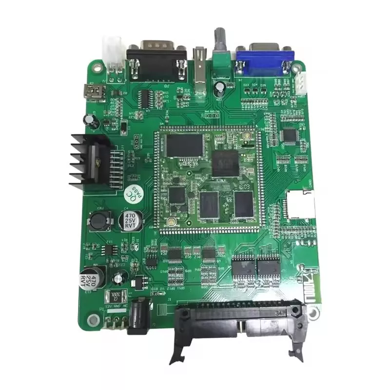
Flex Circuit Board is a revolutionary innovation in circuit board technology. As the name implies, it's a printed circuit board that has been designed to flex, bend and twist without breaking or losing its shape. This flexibility makes it perfect for use in devices that require design adjustments to function correctly.
The Flex Circuit Board is manufactured using high-quality materials that make it highly durable and resilient. It can withstand mechanical, thermal and chemical stress, which makes it the perfect solution for tough environments. The circuit board can also handle high-frequency signals and can be used in a wide range of applications like consumer electronic devices, aerospace, military, and medical devices.
The Flex Circuit Board is incredibly thin, which makes it suitable for use in devices that require compact designs. It is also lightweight, which reduces the overall weight of the device, making it easier to carry around. Flex Circuit Board is highly customizable, with options such as single-sided, double-sided, multi-layered, and rigid-flexible combination options.
Hoshineo Lcd-Tech 4-layer PCB specification :
|
Layer Count(L) |
4 Layers |
Copper Thickness(OZ) |
140um(4OZ) |
|
Production Panel Size(mm) |
≤483*623mm |
Line Width/Space |
3/3mil |
|
Core Thickness(mm) |
0.05 |
Hole Plating Aspect Ratio AR |
≤10:1 |
|
Dielectrict Thickness(mm) |
≧0.005 |
Warpage |
0.60% |
|
BGA Pad Pitch(mm) |
≧0.4 |
SMT Pitch (mm) |
≧0.5 |
|
Solder Mask Regisvation(mm) |
±0.038 |
Impedance Controltolerance |
±8% |
|
Inner Layer Clearance |
≧20 µm |
Surface Treatment |
HASL(lead and lead free),Plating/ENIG,OSP |
Hoshineo Lcd-Tech 4-layer PCB Product Features and functions
Laminated structure: A typical 4-layer PCB stack structure includes a top signal layer, an inner layer 1, an inner layer 2, and a bottom signal layer. This structure provides more flexibility and complexity in circuit design.
Conductive channel: Through the hole to connect different layers of the circuit to achieve signal transmission and component interconnection.
Material selection: Glass fiber or other insulating materials are usually used as the substrate, and the surface is covered with copper foil for wiring.
Signal transmission: The main function of the 4-layer PCB is to act as a medium for signal transmission between electronic components, and connect the various components through wiring to achieve the function of the circuit.
Power distribution: The inner layer can be used as a power layer (VCC) to provide a stable power supply to the circuit.
Ground protection: The inner layer can also act as a ground layer (GND), providing ground protection for the circuit, stabilizing the signal and preventing interference.
Hoshineo Lcd-Tech 4-layer PCB Details
Packaging & shipping
To better ensure the safety of your goods, professional, environmentally friendly, convenient and efficient packaging services will be provided.
